Let’s Etch PCBs!
printed circuit board (PCB): a thin board to which electronic components are fixed by solder
Why bother making a printed circuit board? Well, if you are planning on replicating a circuit design for a more permanent project, then save yourself the trouble of having to build everything from scratch. Why bother making a printed circuit board if you do not want to make anything with electronics? Etching pcbs can be as much of an artistic tool or method as screen printing, you just using different materials. You can achieve a different aesthetic … that can also be a functional electronic circuit.
This how-to is meant for the technological artist who wants to make PCBs in the kitchen, ghetto-style.
Steps involved:
We will present the exposure method for making pcbs, there is an even cheaper method using toner from a laser printer as opposed to photoresist.
We do not have a laser printer available so have not not tried it. Learn more about different methods here.
Dan Wilcox & Oscar Ramos
Interactive Installations 07, C:Art:Media, Valand School of Art, Gothenburg, Sweden
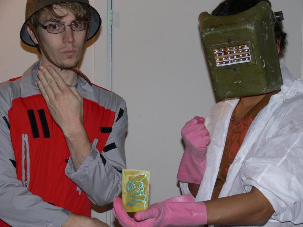
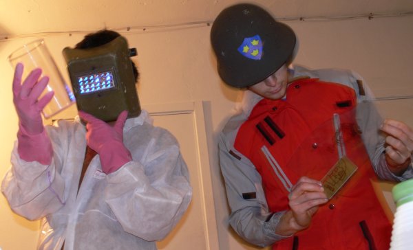
Workshop Pictures
Pictures and Board Designs from Previous Workshops
18nov07 |
25nov07 |
Artistic Example
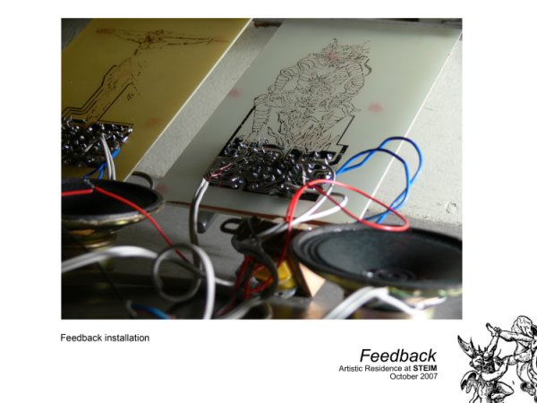
Oscar Ramos built an audio feedback system using inexpensive computer amplifiers and custom circuit boards depicting Jesus and the Devil. In this case, the pcb is both a practical and aesthetic medium.
Check out more information at his STEIM project blog post for the project.
Before we began, we read up on the theory, methods, and materials involved with making pcbs. Also, since we are dealing with non-household chemicals make sure you understand their safe usage and disposal by checking their material safety data sheets (MSDS).
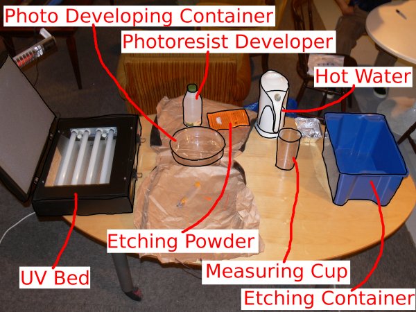
OK, let’s get all of our materials together:
- a plastic transparency sheet
- printed circuit board w/ photoresist (ELFA no. 49-576-68) 1
- powder developer for positive photoresist (20g ELFA no. 49-577-00)
- etching powder, sodium persulfate (150ml ELFA no. 49-577-26) 2
- uv bed, borrowed from work (similar to ELFA no. 49-821-04) 3
- a photo developing container, in our case a glass bowl
- an etching container, in our case a plastic tub
- measuring cup
- hot/boiling water
- rubber gloves
For our sample, we bought the photo and etching chemicals at ELFA and used a blank pcb lying around. Since we are using the uv exposure method, we managed to find a uv bed. For messing with the chemicals, we used glass and plastic containers and rubber gloves to avoid contact with the skin. The sodium persulfate etchent (etching chemical) works best at around 50°C and can be stored and reused safely.
We went ahead and prepared the photo developing solution by mixing the chemical powder with water and placing it in a plastic bottle.

1 The pcb blank we used is of the single-sided variety with one side being coated with the photoresist chemicals.
2 There are 2 types of popular etching chemicals: ferric chloride and sodium persulfate. The former is cheap, dirty, and brown while the latter is pricier, cleaner, and clear. We do not like messy ferric chloride and besides, ELFA does not sell it anyway.
3 We were lucky enough to borrow a uv bed from work to expose the pcb. These things are generally expensive for some reason, even though they are just boxes with fluorescent uv lamps inside. You can make your own inexpensive exposure box using uv bulbs, although it may take longer if the bulbs are not very strong (check the wattage). One other option is direct sunlight, but this is not so useful in the dark Swedish winter! Check out one diy option.
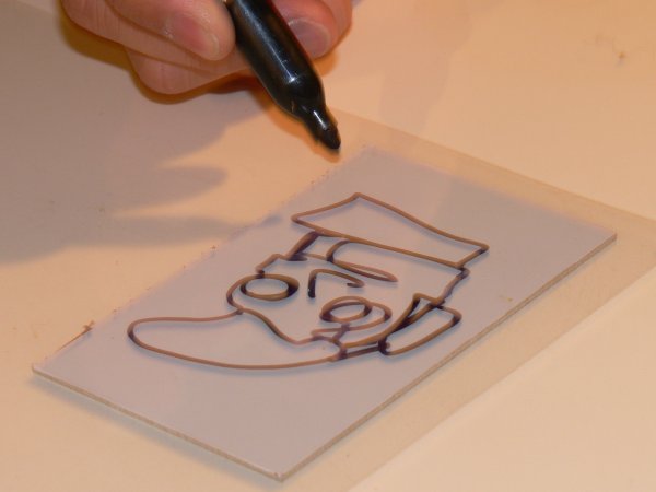
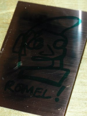
We asked a friend to make a quick drawing for our sample using a black permanent marker.
There are 3 ways to make the design/artwork for your pcb:
- draw the design by hand on the transparency with a black marker
- use photoshop or another digital drawing program to create the design
- use a computer assisted design (cad) program to create the design, such as Eagle
In all cases, the final result you want is the design in solid black on a clear transparency sheet. You want the lines to be as solid as possible, otherwise light might bleed through and the exposure will not be uniform on the pcb. UV exposure will give you good lines (circuit traces) down to about 0.2mm.
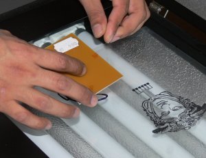
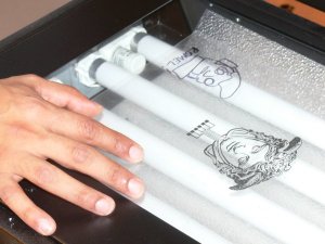
Now remove the plastic film covering photoresist on the pcb and place it over the design on the transparency in the uv bed.
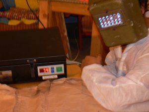
Let it expose for a certain amount of time depending on the strength of your uv light source. You want more exposure time as opposed to too little. We set the uv beds timer to 96 seconds for our setup.
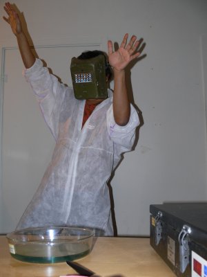
Now that we had some free time, let’s dance!
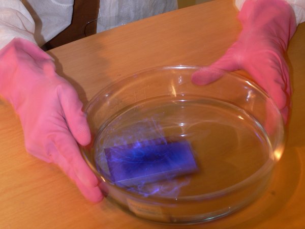
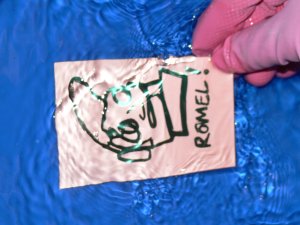
When the exposure is done, place the pcb in the developing solution (which you should have prepared earlier). Slosh it around in the container gently until the design appears as the photoresist is removed.
Your end result should be a pcb with the design on top of a visible copper layer.
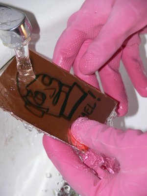
Clean the remaining photodeveloper from the pcb with water.
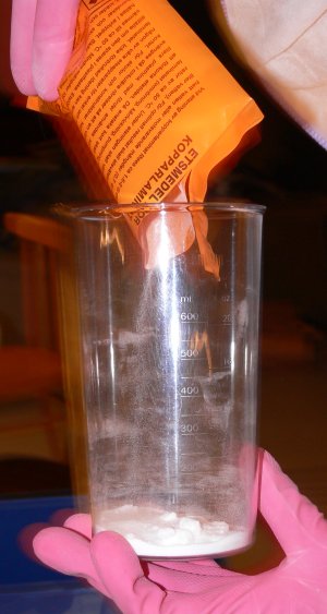
Prepare the etchent powder for mixing with water. Our powder mixes 5:1 with water, so the 1.5 dl packet was good for 1L of solution. Make sure you wear those gloves, as the MSDS for sodium persulfate lists it as a strong oxidizer that may cause burns.
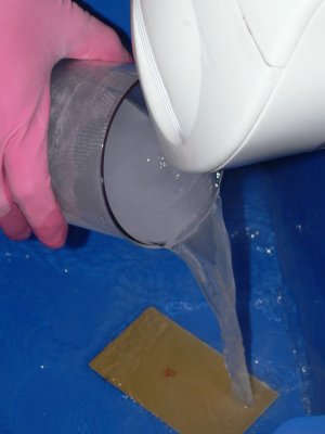
Add the etchent powder with hot/boiling water. The powder should dissolve quickly yielding a light blue solution. Add the pcb to the solution.
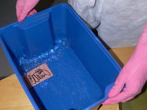
Gently slosh the pcb in the etchent solution which essentially dissolves the exposed copper from the board and leaves the copper under the design. ELFA notes that our powder yields best results at 50°C and only takes about 5 mins to fully etch a board.
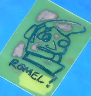
As you watch, the copper will disappear, leaving your design. Make sure you do not etch for too long, as the copper under the edges of the design will begin to dissolve. As you can see in this picture, most of the copper is gone, but the process needs another minute of two.
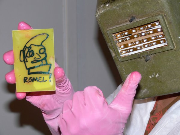
If all went well, you should end up with clean design in copper on a bare board. Our first try failed as our initial drawing was not dark enough on the transparency, so the design did not expose properly. It may take several tries before you come up with the right method depending on the materials you have available.